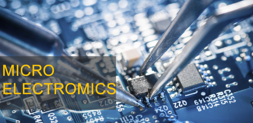
Phtotoetching for Microelectronic devices
As microelectronic products become smaller and smaller to meet customers’ convenience requirements, it has more demand for smaller components. Semiconductor chip connects the world with it. A Photoetching plate as the carrier is the optimal way to supply the flat and burr-free parts. At the same time, it also maintains low tolerance to assure accurate dimensions. Besides the photoetching process avoids most contamination pollution than other production processes. It totally meets the semiconductor requirement on this side.
And we have the flexible tooling to make the goods and modify improves the efficiency. It helps fulfill the aim of producing as many pieces as possible.
Filtalloy has 15 years of professional technique and experience to assure the strong supplying ability and good service. Our superior team has supplied customized solutions to solve different customers’ problems. Meanwhile, we have been keeping learning forefront technology to become the leading company in this industry.
Application: Semiconductor chip for the electronic device
Relevant Product:

Etched Metal
For semiconductor chip of microelectronics industry
fine dimension with lowest tolerance
Less contamination
Inquiry for Our Product
When you contact us, please provide your detail requirements. That will help us give you a valid quotation.
Applications
Request A Quote
Complete our interactive form to receive a custom quote based on your needs.